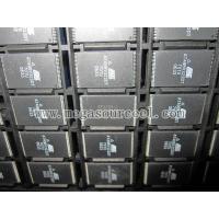
Quick Detail:
DDR2 SDRAM
Description:
The DDR2 SDRAM uses a double data rate architecture to achieve
high-speed operation. The double data rate architecture is
essentially a 4n-prefetch architecture, with an interface designed
to transfer two data words per clock cycle at the I/O balls. A
single readorwriteaccess for the DDR2SDRAM
effectivelyconsistsofasingle4n-bit-wide,oneclock-cycle data
transfer at the internal DRAM core and four corresponding
n-bit-wide, one-half-clock-cycle data transfers at the I/O balls.
A bidirectional data strobe (DQS, DQS#) is transmitted externally,
along with data, for use in data capture at the receiver. DQS is a
strobe transmitted by the DDR2 SDRAM during READs and by the memory
controller during WRITEs. DQS is edge-aligned with data for READs
and center-aligned with data for WRITEs. The x16 offering has two
data
strobes,oneforthelowerbyte(LDQS,LDQS#)andonefortheupperbyte(UDQS,UDQS#).
The DDR2 SDRAM operates from a differential clock (CK and CK#); the
crossing of CK going HIGH and CK# going LOW will be referred to as
the positive edge of CK. Commands (address and control signals) are
registered at every positive edge of CK. Input data is registered
on both edges of DQS, and output data is referenced to both edges
of DQS as well as to both edges of CK.
Read and write accesses to the DDR2 SDRAM are burst-oriented;
accesses start at a selected location and continue for a programmed
number of locations in a programmed sequence. Accesses begin with
the registration of an ACTIVATE command, which is then followed by
a READ or WRITE command. The address bits registered coincident
with the ACTIVATE command are used to select the bank and row to be
accessed. The address bits registered coincident with the READ or
WRITE command are used to select the bank and the starting column
location for the burst access.
The DDR2 SDRAM provides for programmable read or write burst
lengths of four or eight locations. DDR2 SDRAM supports
interrupting a burst read of eight with another read or a burst
write of eight with another write. An auto precharge function may
be enabled to provide a self-timed row precharge that is initiated
at the end of the burst access.
As with standard DDR SDRAM, the pipelined, multibank architecture
of DDR2 SDRAM enables concurrent operation, thereby providing high,
effective bandwidth by hiding row precharge and activation time.
A self refresh mode is provided, along with a power-saving,
power-down mode.
All inputs are compatible with the JEDEC standard for SSTL_18. All
full drive-strength outputs are SSTL_18-compatible.
Applications:
• VDD = +1.8V ±0.1V, VDDQ = +1.8V ±0.1V
• JEDEC-standard 1.8V I/O (SSTL_18-compatible)
• Differential data strobe (DQS, DQS#) option
• 4n-bit prefetch architecture
• Duplicate output strobe (RDQS) option for x8
• DLL to align DQ and DQS transitions with CK
• 8 internal banks for concurrent operation
• Programmable CAS latency (CL)
• Posted CAS additive latency (AL)
• WRITE latency = READ latency - 1 tCK
• Selectable burst lengths (BL): 4 or 8
• Adjustable data-output drive strength
• 64ms, 8192-cycle refresh
• On-die termination (ODT)
• Industrial temperature (IT) option
• RoHS-compliant
• Supports JEDEC clock jitter specification
Specifications:
Datasheets | MT47H512M4,256M8,128M16 |
Product Photos | MT47H64M16HR-25:H TR |
Standard Package | 1,000 |
Category | Integrated Circuits (ICs) |
Family | Memory |
Series | - |
Packaging | Tray |
Format - Memory | RAM |
Memory Type | DDR2 SDRAM |
Memory Size | 2G (128M x 16) |
Speed | 2.5ns |
Interface | Parallel |
Voltage - Supply | 1.7 V ~ 1.9 V |
Operating Temperature | 0°C ~ 85°C |
Package / Case | 84-TFBGA |
Supplier Device Package | 84-FBGA (9x12.5) |
Other Names | 557-1535
MT47H128M16RT-25E:C-ND
MT47H128M16RT25EC |
Competitive Advantage:
Warranty :180days for all goods
Free shipping:Order over $600 win a free shipment fee:goods weight
below 3Kg.
Mega Source Electronics stocks components ready to ship. Hard to
find, obsolete and highly allocated integrated circuits and
semiconductors are all can be found by us.
Mega Source Electronics has established a well-developed logistics
system and global logistics network, which can guarantee our
service very quick, convenient and efficient.


